
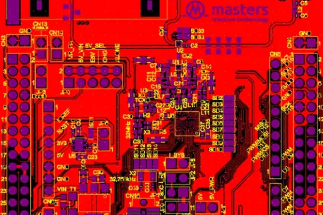
Gerber files are a standardised file format used in the electronics industry for Printed Circuit Board (PCB) designs. Both designers and circuit manufacturers use them to convey information about desired PCB parameters with great precision. Each layer of the PCB is represented by a separate Gerber file. This includes files for the copper layer, solder mask layer, silkscreen layer, drill files and an outline file for the PCB. These files are generated using Electronic Design Automation (EDA) software, such as Altium Designer, KiCad, or Eagle.
Gerber Files – Standards
There are a few Gerber file standards that have evolved alongside increasingly advanced PCB designs.
The most common Gerber file standards are:
- Gerber RS-274-D: a standard that is now being phased out. It required manual aperture definitions, which were provided in a separate file. It was a simple ASCII format consisting only of commands and XY coordinates.
- Gerber RS-274-X: introduced in the 1990s, this is currently the most widely used standard in the electronics industry. It includes all the necessary layer descriptions for PCBs and does not require additional aperture files. The format also supports advanced features, such as polygon fills.
- Gerber X2: introduced in 2014, this standard is an extension of the RS-274-X standard. It includes additional information on layer locations, pads and impedance control. Thanks to this standard, projects can be understood more easily, reducing the need for communication between manufacturers and clients.
Naming conventions for Gerber files in the RS-274-X standard

The extension of a Gerber file defines the layer or function it represents. Using the correct file names reduces the risk of errors occurring during production. Examples of Gerber file extensions are given below. These may differ depending on the EDA program used to prepare the PCB design:
- GTS / GBS - solder mask layer,
- GTL / GBL - copper layer,
- GTO / GBO - Silkscreen layer,
- GKO - PCB outline,
- GM1 - mechanical layer,
- DRL - drill file in Excellon format.
Software solutions for opening Gerber files.
Most EDA software comes with dedicated modules that allow you to view Gerber files after they have been generated. Some of these modules allow you to edit the files to a limited extent after they have been generated. There are also programs that PCB manufacturers use to prepare PCB production using Gerber files received from customers. These programs include Design for Fabrication (DFF) functions that enable you to verify the design against the manufacturer's requirements and detect errors such as failing to connect a track to an SMD pad.
The following are some examples of programmes for handling Gerber files:
- Gerbv: free, open-source tool for verification Gerber files. It is also available for Linux.
- Gerber Viewer module in KiCad: this free PCB design tool includes a module for generating and verifying files. The program supports Gerber X2 files and can display metadata.
- CAMtastic module in Altium Designer: these are the most advanced PCB design tools available, with a built-in module for verifying and editing Gerber files. Using the CAMtastic module, we can prepare a panel for automatic production.
- CAM350: this professional tool is used by PCB manufacturers to prepare for production. The program has design for fabrication features that allow errors to be detected before production begins.
The most common errors in Gerber files

Various complications may arise when generating and sending files to the printed circuit board (PCB) manufacturer, resulting in errors during PCB production or when the module is started up later. The most common errors include:
- Missing layers – This is one of the most common problems and can result in a multilayer PCB being produced with no internal layers or holes if a layer is missing.
- Use of two different units of measurement: using a combination of metric and imperial units for Gerber files and drill holes may result in PCBs being produced with incorrect dimensions, or holes being drilled incorrectly.
- Didn't send stack-up: if we do not include information about the layer stack in the Gerber files, the manufacturer will produce the PCB using standard laminate. This may result in errors occurring during the initial start-up process, for example with the radio track.
Conclusion
Printed circuit boards are becoming increasingly technologically advanced. Using Gerber file standards in the PCB design and manufacturing process helps to ensure that designers receive the printed circuit board they intended.