
In the design process, it is crucial to consider principles that will prevent issues during production, ensure the device's reliability, and enable cost optimization. The designer should pay attention to technological aspects, material availability, and other factors to ensure that the final product is not only functional and durable but also economically viable, with the entire production process running smoothly.
The decision to choose the right electronics assembly technology, such as SMT assembly, THT manufacturing, or hybrid assembly, is critical in the production process. This choice impacts mechanical strength, production efficiency, and overall manufacturing costs.
SMT (Surface-Mount Technology) is ideal for mass production, especially for small to medium-sized components that can be easily placed using automated machines. It allows for a high component density on the PCB. THT (Through-Hole Technology) uses components with legs that pass through holes in the PCB and are soldered on the opposite side of the board. This technology is more suitable for larger components or those that require greater mechanical strength, commonly used in prototyping or rugged environments.
Hybrid assembly, combining both SMT and THT, is useful when the PCB design requires the advantages of both technologies. It is suitable for devices that combine small, delicate components with larger, more durable ones.

For smooth and error-free electronics mounting, it's crucial to carefully plan the layout of components on the PCB. A good design is not only essential for proper assembly but also for future testing and device performance. Ensure that SMT components are positioned in alignment with the production direction to ease automatic soldering. THT components should be separated from the SMT areas to avoid assembly errors. It is also essential to design space for cooling and possible testing, which may require additional room on the board. Proper component placement minimizes the risk of failure and improves production efficiency.
The minimum spacing between components on the PCB is critical for the quality of the assembly. Too small distances can lead to shorts and difficulties in cooling the components. Proper spacing allows for automatic assembly, enabling precise soldering. Optimizing spacing also facilitates easier repairs if faults arise. Larger gaps help during servicing and maintenance of the device. Correct dimensioning and spacing are crucial factors for the final product's quality.
Designing PCBs for high-current applications requires selecting the correct trace thickness and width to ensure their strength and stability during device operation. For components that need high current flows, such as power supplies, trace width should be increased to prevent overheating. Avoid sharp angles in traces, as they can cause issues during manufacturing and affect connection quality. Proper copper thickness and trace design improve the performance and reliability of the whole system.
Panelization is the process of combining several PCBs into one larger panel, speeding up the assembly process for both SMT and THT. Panelization reduces material waste and increases production efficiency by optimizing the wave soldering process. For larger production runs, panelization is particularly beneficial, cutting down production time and reducing costs associated with treating each PCB individually. It’s a great solution when high efficiency and minimal production costs are the goal.

Designing the correct pads and mounting holes is a crucial step in the creation of electronic circuits. Depending on the assembly technology (SMT or THT), the proper pad size and spacing greatly affect soldering quality and connection durability. SMT assembly requires precisely sized pads to ensure good adhesion. Pads should be large enough to allow effective soldering with a wave soldering process but not too large to hinder paste application. Too small pads lead to poor soldering, while overly large pads complicate accurate component placement. THT assembly needs holes sized correctly for the component leads. Avoid too small holes, which can make component insertion difficult, and too large holes, which can lead to poor soldering and weak connections.
Thermal management is essential to prevent component damage and maintain system stability. Large temperature differences during soldering can cause issues. To avoid this, ensure proper mass placement and thermal fill. Use thermal fill areas and ground planes to distribute heat evenly during soldering. For components that generate significant heat, design thermal vias to dissipate the heat efficiently. Ensuring uniform trace widths also helps prevent uneven heat distribution.
Optical Inspection (AOI) is a key quality control process during electronics assembly. A well-designed PCB should allow easy inspection and functional testing of components. Designing with AOI in mind requires placing components so they do not block critical areas to be inspected. Additionally, plan for test points for in-circuit tests (ICT) to check connections within the assembly after mounting.
Choosing the correct materials for PCB production is crucial to ensuring durability, functionality, and resistance to external conditions. Depending on the application requirements, various materials may be more appropriate. FR4 is the most commonly chosen material for standard PCBs because it offers a good balance between cost, durability, and electrical conductivity. For more demanding applications, such as flexible PCBs, polyimides are a better choice, offering flexibility at a higher production cost. For high-power applications that require better heat conductivity, ceramic or metal substrates may be used, providing superior thermal and mechanical properties.

A strong partnership with an electronics assembly manufacturer is key to project success. Before starting production, it’s important to consult with the manufacturer to ensure that Gerber files and BOM lists are correct and include available components. This helps avoid delays and costly corrections.
Novatronik – Your partner in electronics final assembly
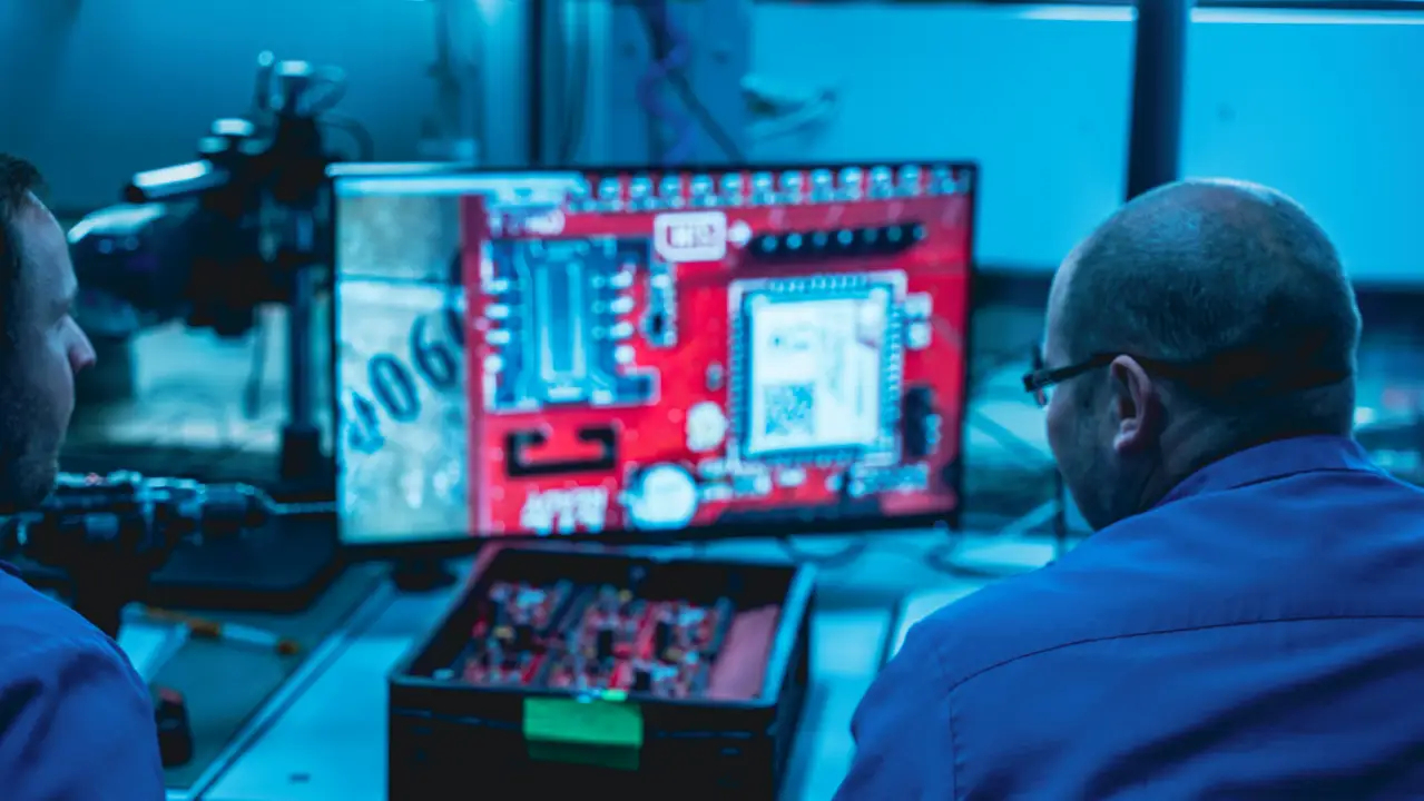
With over 25 years of experience, Novatronik offers comprehensive SMT and THT assembly services, ensuring high-quality results and timely delivery. Our automated production lines, including AOI 3D and X-Ray technologies, ensure precise assembly and complete quality control. Thanks to our flexibility and extensive supplier network, we tailor production to client needs, optimizing costs and lead times.
Want to learn more about our services or discuss your project?
Email us at novatronik@novatronik.com or call +48 506 292 460.
We’re ready to answer your questions and offer the best solutions!
Detailed documentation is essential for smooth assembly and ensuring that connections meet expectations. The documentation should include precise data to help assembly machines complete the project successfully. Production documentation should include:
Before sending the design for production, conduct a detailed Design Rule Check (DRC) to ensure the project meets all technical and manufacturing requirements. DRC helps identify errors that could affect assembly quality. Pay special attention to:
Thoughtful PCB design is the foundation of successful electronics production. Considering appropriate assembly technologies, careful component organization, attention to thermal conditions, and testability are key factors determining the success of the final product. Following the 12 principles discussed in the article ensures the optimization of the design and production process, minimizing the risk of issues during execution. Collaborating with an experienced manufacturer like Novatronik can further streamline the assembly process and guarantee the highest quality of execution.